


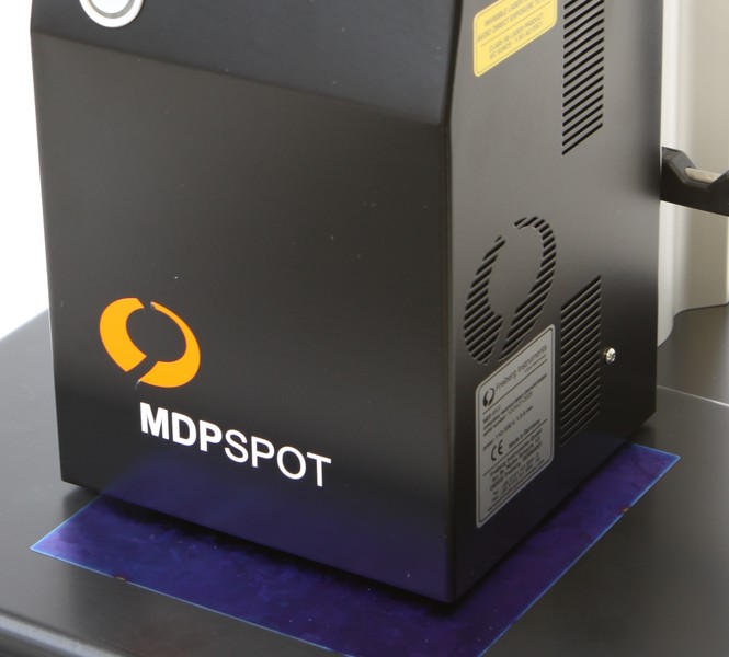
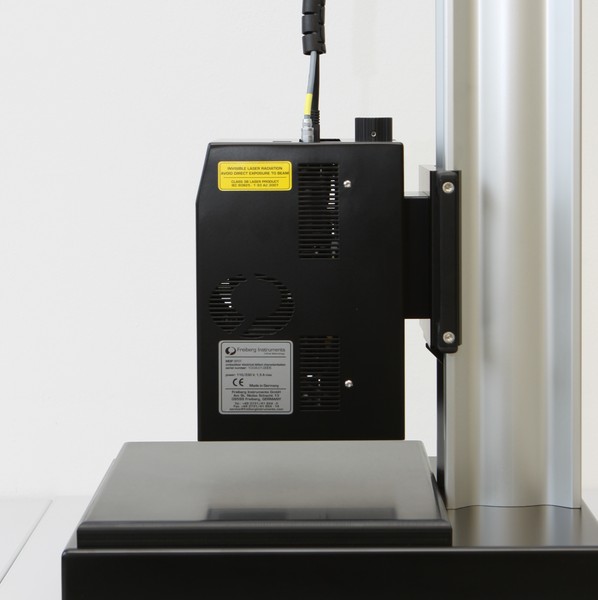
MDPspot


Low cost tabletop single spot measurements on wafers or bricks.
Tabletop single spot measurements
Low-cost tabletop lifetime measurement system for characterization of a variety of different silicon samples at different preparation stages, without built-in automatization. Optional hand operated z-axis for thicker samples up to 156 mm bricks. Standard software for result visualization.
MDPspot w
Includes an additional resistivity measurement option. Resistivity measurements for silicon only, either for wafers without height adjustment possibility, or for bricks. One of these two options has to be predefined.


Facts
-
contactless destruction free electrical semiconductor characterization
-
μ-PCD measurement option included
-
advanced sensitivity for visualization of so far invisible defects and investigations of epitaxial layers
-
integration of up to four lasers for a wide range of injection levels
-
access to primary data of single transients as well as maps for special evaluation purposes
Add-ons
-
Spot size variation
-
Resistivity measurement (wafers)
-
Background/Bias light
-
Reflection measurement (MDP)
-
Software extension
-
Additional lasers
Advantages
-
Tabletop unit for single point measurements of carrier lifetime, multi- or mono-crystalline silicon at different preparation stages, from as- grown up to final devices.
-
Small size, low cost and easy to use. Comes with a basic software for result visualization on a small PC or notebook.
-
Suitable for wafers up to bricks, with easy to handle height adjustment.
Technical specifications
| mono or multi silicon wafers, bricks, cells, wafers after different processing steps like passivation or diffusion | |
| sample size | above 50 x 50 mm² up to 12“or 210 x 210 mm² |
| resistivity | 0.2 - 10³ Ohm cm |
| material | silicon wafers, bricks, partially or fully processed wafers, compound semiconductors and beyond |
| measurable properties | carrier lifetime |
| dimension | 360 x 360 x 520 mm, weight: 16 kg |
| power | 110/220 V, 50/60 Hz, 3 A |
Detail
-
allows for single wafer investigation
-
different recipes for different wafer classes
-
monitoring of material, process quality and stability


